Welcome to Luen Fung Silicone Rubber Mfg., Co


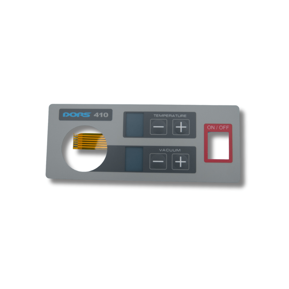
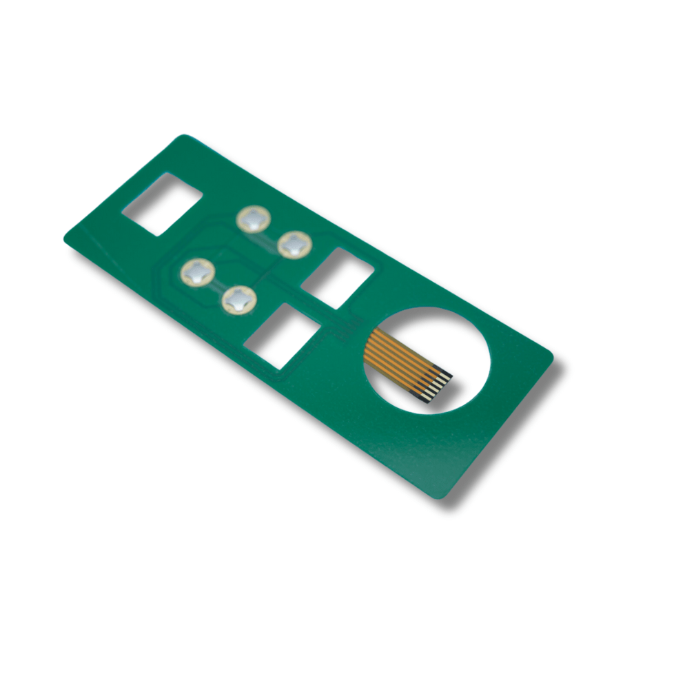
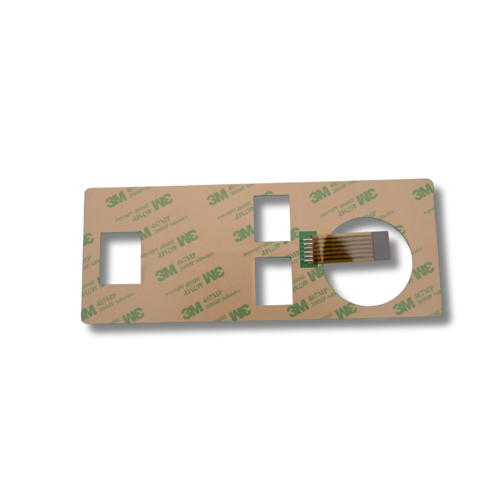


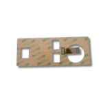
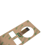
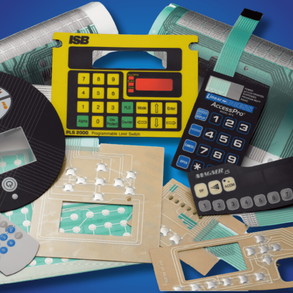
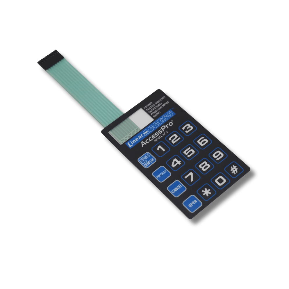
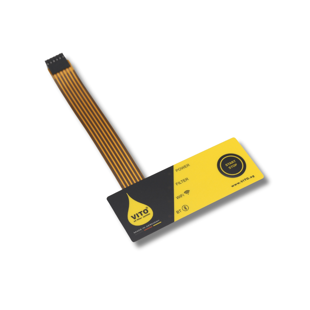
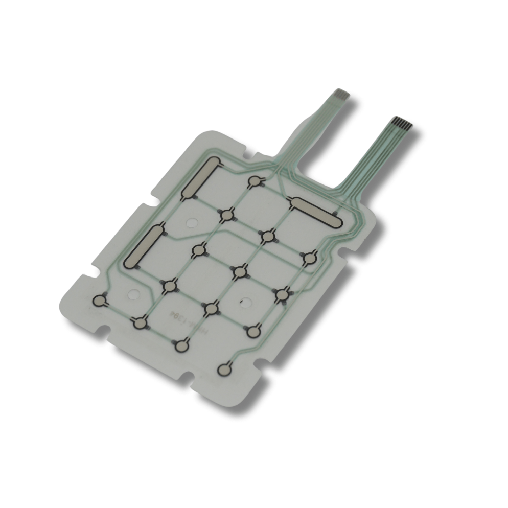
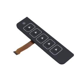
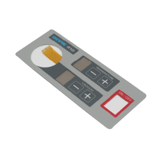
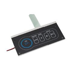
A Printed Circuit Board (PCB) is a crucial component in electronic devices, providing mechanical support and electrical connections for electronic components. Made from a non-conductive substrate, typically fiberglass, with etched copper conductive tracks, PCBs can be single-sided, double-sided, or multi-layered. Components such as resistors, capacitors, and integrated circuits are soldered onto the board. PCBs offer benefits like compact size, reliability, and suitability for mass production. They are widely used in consumer electronics, automotive systems, industrial machinery, medical devices, and aerospace technology, enabling efficient and durable electronic circuit design.
Compact Size: Efficiently organises electronic components, reducing overall device size.
Reliability: Provides consistent and reliable connections, reducing the risk of short circuits and wiring errors.
Mass Production: Facilitates automated manufacturing processes, making large-scale production more efficient and cost-effective.
Durability: Designed to withstand environmental stress and provide long-term performance.
Substrate: Typically made of a non-conductive material like fiberglass or plastic, providing the board’s structural integrity.
Conductive Tracks: Thin layers of conductive material, usually copper, are etched onto the substrate to create pathways for electrical signals.
Components: Various electronic components such as resistors, capacitors, diodes, and integrated circuits are soldered onto the PCB.
Layers: PCBs can have single or multiple layers. Multi-layer PCBs have several layers of conductive traces separated by insulating layers.
Single-Sided PCB: Has one layer of conductive material and is simple and inexpensive.
Double-Sided PCB: Conductive material on both sides of the substrate with vias connecting the two sides.
Multi-Layer PCB: Contains multiple layers of conductive material separated by insulating layers, allowing for more complex and dense circuit designs.
| Material |
| Substrate: Typically FR4 (fiberglass-reinforced epoxy laminate), but also polyimide, PTFE, or other materials for special applications. Copper Thickness: Commonly measured in ounces per square foot (oz/ft²), with standard values being 1 oz/ft², 2 oz/ft², etc. |
| Layer Count |
| Single-Sided: One layer of conductive material. Double-Sided: Conductive material on both sides of the substrate. Multi-Layer: Multiple layers of conductive material separated by insulating layers, with common counts being 4, 6, 8, or more. |
| Board Thickness |
| Standard thicknesses range from 0.4 mm to 3.2 mm, with 1.6 mm being typical. |
| Trace Width and Spacing |
| The width of the copper traces and the spacing between them, which affect the board’s current-carrying capacity and signal integrity. Typical widths and spacings range from 0.1 mm to 0.5 mm, but can be smaller for high-density boards. |
| Hole and Via Specifications |
| Hole Size: Typically ranges from 0.2 mm to 0.6 mm for through-hole components. Vias: Used to connect different layers in multi-layer boards. Types include through-hole vias, blind vias, and buried vias. |
| Surface Finish |
| Common finishes include HASL (Hot Air Solder Leveling), ENIG (Electroless Nickel Immersion Gold), OSP (Organic Solderability Preservative), and others to protect the copper and ensure good solderability. |
| Solder Mask |
| A protective layer applied over the copper traces, typically green, but other colors like red, blue, or black are also used. |
| Electrical Performance |
| Impedance Control: Necessary for high-frequency signal integrity. Current Capacity: Defined by the trace width, thickness, and overall board design. Dielectric Constant (Dk): Of the substrate material, important for high-frequency applications. |
| Thermal Performance |
| Thermal Conductivity: How well the board material dissipates heat. Glass Transition Temperature (Tg): The temperature at which the substrate material changes state, important for high-temperature applications. |
| Mechanical Properties |
| Flexural Strength: Important for boards that will undergo mechanical stress. Dimensional Stability: Ensures the board maintains its size and shape under various conditions. |
*The information & specification are for reference only